How Computers Actually Work: CPU, Memory, and Storage
To effectively reverse engineer binary code, you must approach it not as a puzzle, but as a living system.
Code follows a distinct life cycle: it resides on disk, becomes active in memory, and either concludes its process or is saved to storage. By tracking this progression, you can anticipate, identify, and disrupt malicious activities.
A fundamental understanding of a computer's core components is crucial for comprehending how these intricate machines operate. This document will clarify the functions of the Central Processing Unit (CPU), Memory (RAM), and Storage, detailing their individual roles and their collaborative efforts in executing tasks and managing data.
Why this matters - fast, to the point
- Reverse engineering is tracing intent through layers: bytes -> instructions -> memory -> hardware -> artifacts.
- Malware attacks these layers directly - injection, persistence, timing, and I/O are hardware-aware.
- Mistakes in basic systems thinking lead to wasted reversing effort. Know the platform, then debug the behavior.
The Motherboard: The System's Backbone
The Motherboard, also known as the mainboard or system board, is the primary circuit board of a computer. It acts as the central communication hub, physically connecting and allowing communication between the CPU, RAM, and all other hardware components (like graphics cards, storage drives, and peripherals).
Anatomy of the Motherboard
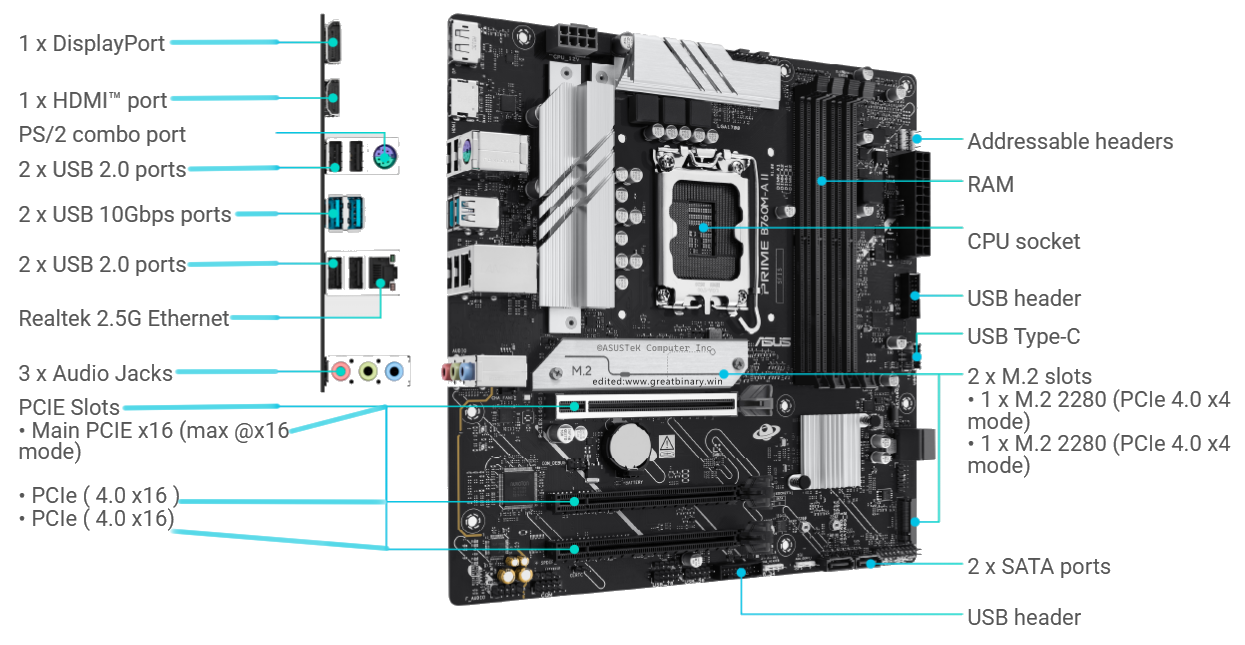
Credit: Diagram adapted from ASUS’s official documentation for the PRIME B760M-A II-CSM motherboard. Used for educational/reference purposes only. All trademarks belong to their respective owners.
-I love you ASUS, please don’t DMCA me.
Motherboard Anatomy: Detailed I/O Ports and Connections
The following list itemizes common connectors and components found on a high-performance motherboard, providing practical examples of the I/O mechanisms discussed (connections to the CPU, RAM, and storage).
# | Component | Function | Relevance to Reversing/Forensics |
1 | DisplayPort | Digital video output for high-resolution monitors; supports adaptive sync and daisy-chaining. | Output artifact; can be exploited via hardware attacks (e.g., monitor spoofing). |
2 | HDMI Port | Digital video and audio output; widely compatible, mainly for TVs and general monitors. | Similar output artifact potential as DisplayPort. |
3 | PS/2 Combo Port | Legacy connector for older keyboards/mice. Used for pre-OS environments like BIOS. | Can be used for low-level interaction or stealthy keylogging (pre-OS). |
4, 6, 13, 17 | USB 2.0/Headers | Low-speed USB connections (480 Mbps) for basic peripherals and case front ports. | Common vector for malware delivery (flash drives) and basic peripheral logging. |
5, 14 | USB 10 Gbps (USB 3.2 Gen 2) | High-speed ports (10 Gbps) for external storage (SSDs) and VR devices. | Faster data exfiltration or rapid external access. |
7 | Realtek 2.5 G Ethernet | Integrated network interface supporting up to 2.5 Gbps wired speeds. | Primary path for network communication, C2 traffic, and network persistence. |
8 | 3 × Audio Jacks | Standard 3.5 mm analog ports (Line out, Line in, Mic in). | Potential vector for data exfiltration via ultrasonic communication or recording environment audio. |
9 | PCIe Slots | High-speed expansion slots (x16 for GPU, x4 for others). | Allows for kernel-level persistence via hardware (e.g., dedicated NICs, custom cards). Direct line to the CPU/chipset. |
10 | Addressable Headers | 3-pin ARGB connectors for controllable RGB lighting. | Generally low-level, but can sometimes be manipulated for side-channel attacks (uncommon). |
11 | RAM Slots (DDR5 DIMM) | Holds RAM modules; supports dual-channel configuration. | Directly relevant to Memory (RAM) section. Physical location where active code and data reside. |
12 | CPU Socket (LGA 1700) | Physical connection for the CPU. | Directly relevant to CPU section. The physical brain of the execution pipeline. |
15 | 2 × M.2 Slots | Slots for PCIe 4.0 ×4 NVMe SSDs. M.2_1 often direct to CPU; M.2_2 to chipset. | High-speed Storage vector. Faster read/write persistence path for malware. |
16 | 2 × SATA Ports | Legacy connectors for SSDs/HDDs (up to 6 Gbps). | Traditional Storage vector. Often shares lanes with M.2 slots (a resource conflict to note). |
Essential Motherboard Components and Concepts
Chipset
The Chipset is a set of integrated circuits on the motherboard that manages data flow between the CPU, memory, and peripherals. It is typically divided into two parts:
- Northbridge (or Memory Controller Hub): Historically managed high-speed components like the CPU, RAM, and graphics card (via the PCIe slot). In modern CPUs (like recent Intel and AMD), this functionality is often integrated directly into the CPU itself.
- Southbridge (or I/O Controller Hub): Manages slower peripherals and I/O functions, including USB, SATA ports (for storage), audio, and the BIOS.
Firmware: BIOS/UEFI
Firmware is a specialized class of software that provides low-level control for the computer's hardware. The two primary types are:
- BIOS (Basic Input/Output System): The traditional firmware interface. Its main job is the POST (Power-On Self-Test), which checks all hardware components. It then loads the bootloader from a storage device to start the operating system.
- UEFI (Unified Extensible Firmware Interface): The modern successor to BIOS. UEFI offers faster boot times, support for larger hard drives (GPT partitions), and more advanced security features.
From a reversing perspective, understanding the firmware is key because rootkits and low-level malware (like bootkits) often target this layer to achieve maximum persistence and stealth, as they execute before the operating system's security features load.
CMOS Battery (Complementary Metal-Oxide Semiconductor)
The CMOS battery is a small, coin-sized battery on the motherboard. Its function is to provide power to a small, persistent memory chip (the CMOS chip) even when the computer is unplugged. This chip stores critical system information, including:
- Date and time.
- System hardware configuration details.
- The current BIOS/UEFI settings.
Key Motherboard Connections
The motherboard is covered in various slots, ports, and connectors that facilitate component communication:
Connection Type | Function | Connected Component/Device |
CPU Socket | Physical and electrical connection for the CPU. | Central Processing Unit (CPU) |
RAM Slots | Holds and electrically connects the RAM modules to the CPU/Chipset. | Random Access Memory (RAM) |
PCIe Slots | High-speed slots for expansion cards (e.g., graphics cards, network adapters). | GPU, Network Cards, SSDs |
SATA Ports | Interface for connecting storage devices. | Hard Disk Drives (HDD), Solid State Drives (SSD) |
USB Headers | Internal ports for connecting case-mounted USB ports. | External Peripherals |
Power Connectors | Receive power from the Power Supply Unit (PSU). | PSU (24-pin ATX, 8-pin EPS) |
Low-Level Hardware Communication Overview
- CPU ↔ RAM Communication
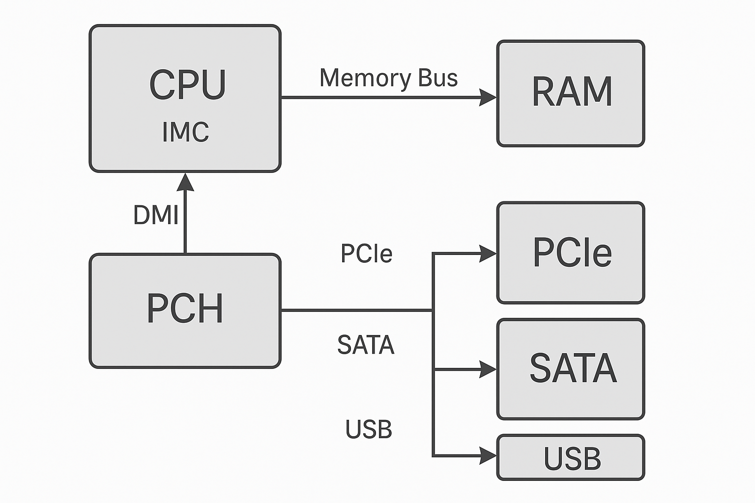
The CPU talks to RAM through the Integrated Memory Controller (IMC), which is inside the CPU die on modern Intel chips.
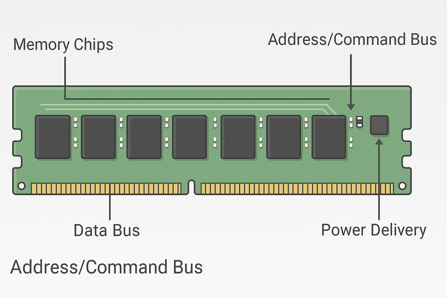
The link between the CPU and the DIMM slots is the memory bus - a direct, high-speed channel with separate lines for:
- Address bus → which memory cell to access.
- Data bus → the actual bits being read or written.
- Control lines → timing, read/write commands, and chip-select signals.
Each "channel" in dual-channel memory doubles theoretical bandwidth.
For DDR5, memory transactions occur in bursts, each clock tick transferring multiple words (burst length = 16).
From an assembly or RE standpoint:
A MOV from memory to a register (MOV RAX, [RBX]) ultimately triggers a load request through the L1/L2/L3 cache hierarchy, and only if missed, a DRAM transaction across this memory bus.
You never "see" that bus in code - it’s abstracted by the cache controller logic - but latency and alignment still matter in performance profiling.
- Internal Buses and Hierarchy
a. System Agent / DMI
The CPU connects to the chipset (PCH) using the Direct Media Interface (DMI) - a PCIe-based internal link (PCIe 4.0 ×4 on this board).
This carries I/O traffic: SATA, USB, Ethernet, audio, etc.
Think of it as the "northbridge–southbridge" successor:
- Old systems had separate chips; now the CPU absorbed the northbridge (memory controller + PCIe lanes).
- The PCH is the modern southbridge.
b. PCIe (Peripheral Component Interconnect Express)
The GPU, NVMe drives, and expansion cards use PCIe lanes (point-to-point serial links).
Each lane transmits differential pairs for data in each direction.
PCIe is packet-based - transactions are TLPs (Transaction Layer Packets), not parallel address/data lines like legacy PCI.
Assembly relevance: device memory mapped through MMIO regions, visible to you in ring-0 via physical address ranges (e.g., GPU BAR0).
- CPU ↔ PCH (Chipset) Traffic
PCH handles "slower" peripherals (USB, SATA, network).
The CPU routes all those through DMI, which has much less bandwidth than PCIe ×16 for the GPU.
Reverse engineers tracing driver behavior often see reads/writes to MMIO regions that are, in fact, chipset register accesses tunneled via DMI.
- Interrupts & Event Signaling
The old INT lines (physical interrupt wires) were replaced by APIC (Advanced Programmable Interrupt Controller).
Devices now send interrupts over the bus (MSI/MSI-X), not via pins.
In RE, you might see mov eax, cr8 or sti/cli instructions controlling interrupt masking.
These map to APIC registers at physical addresses (e.g., 0xFEE00000).
- BIOS/UEFI and Initialization Path
On power-on, the CPU starts in real mode (16-bit), executing firmware from the SPI-ROM chip attached via the PCH.
The BIOS initializes RAM timings, PCIe enumeration, and sets up the APIC tables.
For reverse engineers studying bootkits or firmware implants, these early memory-mapped regions are critical (e.g., SPI flash mapped at 0xFF000000 range).
- Clock and Timing Domains
Every data transfer (RAM, PCIe, DMI) relies on synchronized clock domains.
The CPU has an internal PLL (phase-locked loop) generating multiple frequencies.
Reverse engineering timing behavior or analyzing side-channels (cache timing, DRAM rowhammer) means understanding how these domains drift and synchronize.
- Power Planes and Control
The CPU’s power delivery comes through VRMs (Voltage Regulator Modules) next to the socket.
They’re controlled via SVID (Serial Voltage ID) - a digital link between the CPU and VRM controller.
Attackers have used this interface for undervolting-based exploits (e.g., Plundervolt).
- Memory Map Summary (Simplified)
Region | Typical Range | Description |
0x00000000–0x0009FFFF | Real-mode RAM / BIOS data | |
0x000A0000–0x000FFFFF | Video memory, legacy | |
0x00100000–Top of RAM | Main system RAM | |
0xF0000000–0xFFFFFFFF | MMIO: PCIe devices, APIC, BIOS ROM |
-For RE, this mapping is how `MmMapIoSpace` or `/dev/mem` gives access to hardware registers directly.
- Debug/Reverse Engineering Angles
- PCIe sniffing: hardware analyzers can capture packets on GPU or NVMe lanes.
- DMA access: bus mastering devices can read arbitrary RAM if IOMMU isn’t configured - common exploit vector.
- Microcode updates: applied through MSRs (wrmsr instruction), affecting instruction behavior dynamically.
- SMBus/I2C: low-speed serial bus for sensors, VRM control, and SPD EEPROMs on RAM - useful for firmware extraction.
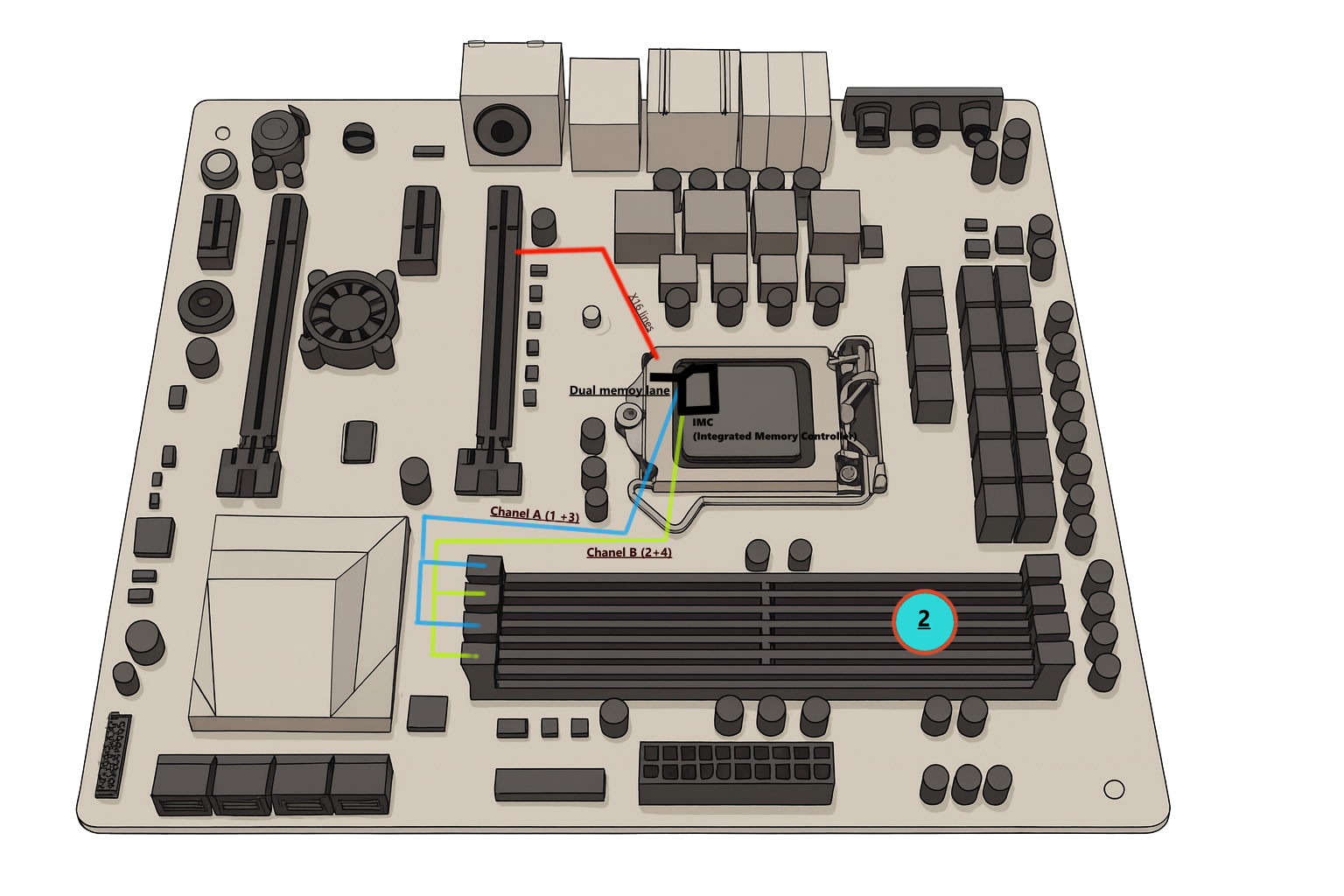
- IMC (Integrated Memory Controller)
The IMC sits inside the CPU and handles all DRAM access. It manages timing, refresh cycles, and parallelism across the two memory channels.
IMC Timing and Security Relevance
The IMC controls the precise electrical timing of DRAM operations, including refresh cycles.
- Refresh Cycles: DRAM cells are capacitors that leak charge, requiring periodic 'refresh' operations by the IMC to retain data. This process is highly predictable and is what enables:
- Cold Boot Attacks: By quickly removing power and cooling the RAM modules, data remanence can persist for several minutes (as the leakage rate slows). The attacker then reads the memory contents before the remaining charge decays.
- Timing Attacks: Predictable refresh timing can be exploited in side-channel attacks by measuring the time difference in memory access between cached and non-cached data, potentially leaking cryptographic keys or other sensitive information.
- RowHammer: This exploit targets the physical structure of DRAM chips. By rapidly accessing (hammering) memory cells in one row, the high-voltage activity can cause charge leakage in adjacent rows, potentially flipping bits (0 to 1, or 1 to 0). This is a physical security fault managed entirely by the IMC's scheduling and address mapping logic.
- Dual Channel Architecture
The CPU accesses two independent 64-bit channels (Channel A and B). Each can read/write simultaneously, effectively doubling bandwidth.
- Channel A → DIMM slots 1 and 3
- Channel B → DIMM slots 2 and 4
When one channel stalls on latency, the IMC can issue operations to the other.
- Data Path (Bus)
Each channel carries a data bus (DQ), address bus (ADDR), and command bus (CMD).
- The data bus transfers the payload (the bytes you read/write).
- The address bus tells the DRAM which row/column to open.
- The command bus issues signals like READ, WRITE, PRECHARGE, or REFRESH.
- Instruction-Level Implication
When assembly code executes MOV [mem], reg, the CPU pipeline issues a load/store micro-op, which triggers the IMC to perform a DRAM transaction if the data isn’t cached.
Caches buffer the request, but the physical memory access still travels through these exact channels. - Signal Timing
DDR5 transfers 16 bursts per clock, and the IMC uses multiple sub-channels to manage command efficiency. That’s why memory latency and clock synchronization directly affect reverse-engineered timing results.
Memory (RAM)
If the CPU is the brain, RAM is its working memory.
Random Access Memory (RAM) is a type of volatile memory that the CPU uses to store data and instructions that are currently being used. It's called "random access" because the CPU can quickly access any piece of data directly, rather than having to read through it sequentially.
Characteristics of RAM:
- Volatile: Data stored in RAM is lost when the computer is turned off.
- Fast Access: RAM is significantly faster than storage devices, allowing the CPU to retrieve data quickly for processing.
- Multitasking: More RAM allows a computer to run more applications simultaneously without slowing down.
Component | Description | Speed | Volatility |
RAM | Temporary storage for active data | Very Fast | Volatile |
Memory is where code runs, communicates, and hides. It is layered and virtualized.
- Hierarchy - Registers -> L1/L2/L3 Cache -> RAM -> Swap -> Disk. Speed falls as capacity grows.
- Virtual memory - each process gets a private address space. Pages are mapped, protections applied (RX/RW/X).
Memory is layered by speed:
[Registers] → [L1/L2/L3 Cache] → [RAM] → [Disk]
Memory Layout of a Process
Every process has its own virtual memory space divided into regions:
[ High addresses ]
Stack - grows down
----
Heap - dynamic allocations (malloc/new)
----
Data - globals, statics
Code - executable sections (.text)
[ Low addresses ]
Core Memory Concepts
- Memory Cell: The fundamental circuit component for storing a single bit of data.
- Memory Word: A collection of bits, typically ranging from 8 to 64.
- Byte: A specific unit defined as a group of 8 bits.
- Capacity (Density): The measure of the total information storage capability of the system.
Capacity Example
A memory system with 4096 memory words, each 20 bits long, has a total storage capacity of 81,920 bits (calculated as 4096 words x 20 bits/word, or 4k X 20).
Note: The discussion on Addresses and Operations is introduced with the example of an 8-word memory system, but the details are not expanded upon in this section.
Addresses | Word |
|
|
|
|
|
|
|
|
|
|
|
|
|
|
|
|
Read and Write Operations
The fundamental interactions between the CPU and memory are defined by two operations:
- Read Operation (=Fetch Operation): The process of retrieving data from a specific memory address.
- Write Operation (=Store Operation): The process of saving data to a specific memory address.
Computer Memory: Structure, Addressing, and Operations
Computer memory is fundamentally organized around the concept of a memory location, each assigned a unique identifier known as an address. The smallest unit of memory is the cell, which stores one bit of information (a D-FF, for instance, is a 1-bit memory).
Bits are grouped into larger units called memory words to carry meaningful information. Standard word sizes include 8-bit, 16-bit, 32-bit, and 64-bit, though other sizes are possible. The most common word size is the byte, which is an 8-bit word. For example, the ASCII character ‘#’ is represented by the byte value 0x23 (the 0x prefix indicates a hexadecimal number).
Memory Capacity and Organization
The total amount of memory on a chip, or its memory capacity, is commonly measured in kilobits (kb), megabits (Mb), gigabits (Gb), or terabits (Tb). However, these bits can be organized in various ways. For instance, an 8Mb memory chip could be configured as:
- 1 million (1M) words of 8 bits each.
- 2 million (2M) words of 4 bits each.
- 8 million (8M) storage locations of 1 bit each.
The number of unique words in a memory module directly determines the addressing requirement - specifically, the number of address bits needed to uniquely specify every single location.
Memory and Protections:
- Pages and Protections: Memory is organized into pages with various protections (execute-only, read-only, read-write). Modifying these protections (e.g., using VirtualProtect) is a common technique for shellcode to become executable.
- ASLR (Address Space Layout Randomization): This security feature shifts base addresses to make exploit development harder. Bypass strategies often rely on information leaks or predictable pointer values.
- Cache Effects: Side-channel and timing attacks often exploit the behavior of CPU caches.
Malware Tactics to Watch:
- Process Injection: This involves techniques like WriteProcessMemory combined with CreateRemoteThread, Asynchronous Procedure Calls (APCs) or QueueUserAPC, or Return-Oriented Programming (ROP) chains to inject malicious code into legitimate processes.
- Reflective Loading: A method where a Portable Executable (PE) image is mapped directly into memory, and its imports are resolved manually, leaving no disk artifact.
- Heap Spraying: Flooding the heap with payloads to increase the probability of a successful exploit by making the payload's location more predictable.
For Reverse Engineering:
When analyzing memory-related issues, break down your questions into:
- Where are the bytes located?
- Which process or component mapped them?
- What protections are applied to this memory region?
- How were these memory protections or contents changed?
When malware injects code into another process (like svchost.exe), it’s simply writing bytes into one of these memory spaces and telling the CPU to execute them.
The Central Processing Unit (CPU)
The CPU, often called the "brain" of the computer, executes instructions, performs calculations, and manages information flow. Its speed and efficiency are crucial for overall computer performance. While deterministic rather than intelligent, this very determinism serves as a powerful tool.
Central Processing Unit (CPU) - Core Functions and Operations
How Computers Actually Work: The CPU, Memory, and Storage Deep Dive
The Central Processing Unit (CPU) is the engine and brain of the computer system, relentlessly executing instructions and managing all fundamental operations. It is a highly complex, multi-stage pipeline where macro-instructions - the human-readable assembly instructions - are translated into low-level micro-operations (micro-ops). These micro-ops are then dynamically reordered, optimized, and executed out-of-order to maximize efficiency, a feature known as speculative execution. It is this very mechanism of speculative execution and the shared, cached data during reordering that introduces vulnerabilities like Spectre and Meltdown, opening the door for side-channel attacks that leak protected data.I. The Architecture of the CPU
The CPU is an intricate piece of hardware composed of several critical functional units that work in concert:Key Components:
- Arithmetic Logic Unit (ALU): The ALU is the computational core. It is solely responsible for performing all arithmetic calculations (e.g., addition, subtraction, multiplication, division) and all logical comparisons (e.g., AND, OR, NOT, checking for equality or greater than). The speed and efficiency of the ALU dictate the raw processing power of the system.
- Control Unit (CU): Often described as the orchestra conductor, the CU is responsible for directing and coordinating the vast majority of computer operations. It fetches instructions from memory, interprets their meaning (decoding), and then generates the necessary timing and control signals to execute them across the other CPU components, managing their sequential execution flow.
- Registers: Registers are the smallest, fastest, and most critical type of memory, located directly inside the CPU itself. They temporarily hold data, memory addresses, and instructions that are currently being processed. Because they are part of the CPU's immediate workspace, accessing them is vastly faster than accessing the L1 cache or main RAM.
II. The CPU Instruction Cycle
The fundamental operational rhythm of the CPU is governed by the classic Instruction Execution Process, often referred to as the Fetch-Decode-Execute Cycle. This process, while heavily optimized and often occurring in parallel across multiple cores, operates with a single-threaded logic at the micro-level:
- Fetch: The Control Unit retrieves the next instruction from the main memory (RAM) location pointed to by the Instruction Pointer (RIP) and loads it into an instruction register.
- Decode: The instruction is translated into micro-ops. The Control Unit determines the type of operation required (e.g., a load, a store, an addition) and identifies the required operands (data) and registers.
- Execute: The actual operation is performed. The ALU executes the instruction (e.g., performing the addition), data is moved between registers, or data is loaded/stored from/to memory. The result is typically stored in a register.
III. The Role of CPU Registers in Program Flow
Registers act as the CPU's immediate, high-priority workspace, providing critical insights into the processor's current operational state and the data it is actively manipulating. Their contents are paramount when analyzing program execution and control flow.Key Registers for Program and Data Manipulation:
- General-Purpose Registers (GPRs) (e.g., RAX/RBX/RCX/RDX - in x64 architecture): These are flexible registers used by the CPU for temporary storage of data, variables, intermediate results, and sometimes memory addresses. They are the primary locations for data manipulation during program execution.
- Instruction Pointer (RIP/EIP/PC - Program Counter): This register is the absolute key to program control. It stores the memory address of the next instruction to be executed. Any alteration to the RIP - whether intentional (via control flow instructions like branches, function calls, and returns) or unintentional (via an exploit) - directly and immediately changes the entire flow of execution. Corrupting this register is the primary goal of many security exploits as it allows an attacker to seize control over which code the CPU executes next.
- Stack Registers (RSP/RBP - Stack Pointer and Base Pointer): These registers manage the Call Stack, a fundamental data structure in computing. The stack is used to:
- Store local variables for functions.
- Save the state of the CPU (registers) before a function call.
- Crucially, store the Return Address - the RIP value the program must jump back to after a function completes.
- Exploits like Buffer Overflows often target the stack to overwrite the saved Return Address, making the RSP/RBP registers critical for defense and exploitation analysis.
- FLAGS Register (RFLAGS/EFLAGS): This register contains individual bits that are set as a side effect of arithmetic and comparison operations performed by the ALU. These flags (e.g., Zero Flag, Carry Flag, Sign Flag) are subsequently read by conditional branch instructions to make decisions and determine program flow (e.g., "If the Zero Flag is set, jump to address X").
Practical Reversing Note: When you will be utilizing a debugger like x64dbg or IDA Pro to single-step through assembly code, you are not just watching lines of text; you are directly observing the CPU's tiny, rapid heartbeat. By understanding the purpose, contents, and lifetime of these registers, along with the specific calling conventions that dictate how functions pass arguments and manage the stack, a reverse engineer can effectively translate low-level assembly language instructions back into the high-level intent and logic of the original program.
Storage
Storage refers to the components that hold data persistently, even when the computer is powered off. Unlike RAM, storage devices are designed for long-term data retention.
Storage: The Persistent Layer
Storage is the foundational layer where data persists across power cycles, making it crucial for forensic investigations.
- Types:
- HDD (Hard Disk Drives): Traditional spinning platters.
- SSD (Solid State Drives): Faster flash-based storage.
While physical differences impact wear, timelines, and low-level attacks, from a reverse engineering perspective, the file system and loader behavior are more significant.
- File Formats:
- PE (Portable Executable): Used in Windows.
- ELF (Executable and Linkable Format): Used in Linux.
Loaders interpret headers, map sections into memory, resolve relocations, and manage imports for these formats.
- Persistence Vectors: Malware leverages various mechanisms to ensure survival after reboots. These include:
- Services
- Scheduled tasks
- Registry Run keys
- Startup folders
- Drivers
- WMI (Windows Management Instrumentation)
- MBR/UEFI (Master Boot Record/Unified Extensible Firmware Interface)
Each method leaves unique artifacts and timestamps that aid in detection and analysis.
- Evidence: The "footprints" left by malware are critical for understanding its actions:
- Dropped binaries
- Modified configuration files
- Signed drivers
- Corrupted boot sectors
Comparison of Storage Types:
Feature | Hard Disk Drive (HDD) | Solid-State Drive (SSD) |
Speed | Slower | Faster |
Durability | Less durable (moving parts) | More durable (no moving parts) |
Cost | Lower per GB | Higher per GB |
Power Consumption | Higher | Lower |
Key Reversing Tip: Identifying how a binary achieves persistence often reveals its Tactics, Techniques, and Procedures (TTPs). For instance, a signed driver suggests kernel-level components, while MBR modification points to boot-time capabilities.-----From Disk to Execution: A Step-by-Step Overview
When a user initiates a program (e.g., by double-clicking a binary), the following sequence of events typically occurs:
- File Reading & Parsing: The Operating System (OS) reads the binary from storage, performing initial parsing (e.g., extracting the DOS and NT headers for a PE file).
- Memory Mapping: The loader maps different sections of the binary into virtual memory. For example, the .text section (containing executable code) is mapped to executable pages, while the .data section (containing initialized data) is mapped to read/write pages.
- Import Resolution: The loader resolves external functions (imports) required by the binary, often through mechanisms like LoadLibrary and GetProcAddress, unless the binary handles this manually.
- Relocation Application: If Address Space Layout Randomization (ASLR) has altered the binary's base address in memory, relocations are applied to ensure correct memory access.
- EntryPoint Execution: The program's EntryPoint is executed, initiating constructors, initializers, and ultimately the main function.
- Runtime Activity: Following the EntryPoint, the program begins its dynamic operations, including heap allocations, thread creation, and file operations. These activities offer further opportunities for inspection and analysis.
Defensive Interception: Defenders actively work to intercept or emulate any of these execution steps to analyze or disrupt malicious activity.
SSD vs HDD: How Data is Written and Destroyed
Not all storage is created equal.
HDDs and SSDs behave completely differently at the physical level - and understanding how they write and delete data determines whether something can be forensically recovered or permanently lost.
1. How HDDs Write and Delete Data
A Hard Disk Drive (HDD) stores data magnetically on spinning platters.
Each sector represents binary states (north/south magnetic orientation = 0/1).
- Write: When you save a file, the disk head moves over the platter and magnetizes sectors to encode the new data.
- Delete: When you delete a file, nothing is actually erased.
The operating system only marks those sectors as “free” in the filesystem table.
The raw bytes remain untouched until something overwrites them. - Result:
Because the old magnetic patterns persist, forensic tools can read them - sometimes even after one overwrite, due to magnetic remanence.
This is why data carving, file recovery, and forensic reconstruction work so well on HDDs.
Forensic implication:
“Deleted” on HDD means “ignored,” not “gone.”
Tools like photorec, foremost, or deep hex carving simply bypass the filesystem and read the marked sectors directly.
2. How SSDs Write and Delete Data
A Solid-State Drive (SSD) stores data as electrical charges in NAND flash cells.
These cells wear out over time, so the drive’s controller spreads writes across memory blocks using wear leveling.
- Write: Data is written in pages (usually 4–16 KB). But flash memory can only be erased in entire blocks (typically 256–512 pages).
That means modifying one small file forces the controller to write new pages elsewhere and mark the old block as stale. - Delete: When you delete a file, the OS flags the logical address as “free,” but the SSD immediately receives a TRIM command.
The Flash Translation Layer (FTL) inside the SSD manages physical-to-logical mapping and wear leveling. This means forensic tools can’t directly correlate logical addresses to real memory cells - the FTL abstracts them entirely TRIM tells the controller to electrically erase those cells in the background, so the next write is faster.
Once TRIM is executed, recovery is practically impossible - the physical charge pattern is destroyed.
Forensic implication:
SSDs actively destroy deleted data as part of normal operation.
Once TRIM executes, no software recovery is possible without a controller exploit or chip-level access.
3. Data Retention and Power Loss
HDDs are magnetic - data persists for decades if the platters aren’t damaged.
SSDs, however, rely on trapped electrical charge inside floating gates:
- When power is lost, that charge slowly leaks.
- Over months or years, cells lose their stored electrons, especially under heat.
- Eventually, bits flip unpredictably - data corruption or total loss.
This is known as data retention decay.
Consumer-grade NVMe drives can start losing integrity after a few months of being unpowered; enterprise SSDs retain data longer but still degrade without refresh cycles.
(Data retention estimates: consumer SSDs ~1 year unpowered at 30°C; enterprise drives up to 5 years depending on NAND type.)
In short:
HDDs rot mechanically. SSDs rot electrically.
One can be recovered with magnets, the other fades silently with time.
Hard Disk Drive (HDD): Magnetic Recovery
HDDs store data on spinning magnetic platters. Data is written by an actuator arm moving a read/write head over the platter, which magnetically aligns tiny areas on the surface (representing bits).
- Writing Data: The write head changes the polarity of the magnetic material on the platter surface. When a file is modified, the OS typically instructs the write head to write the new data to a new location or overwrite the old location on the platters.
- Deleting Data (Logical Deletion): When a file is "deleted" in the operating system (e.g., emptied from the recycle bin), the OS does not immediately erase the data on the platters. Instead, it marks the file's entry in the File System Table as free, making that space available for new data. The magnetic data remains on the platter until a new file overwrites it.
- Forensic Implication: Due to logical deletion, forensic investigators can often recover deleted files by directly reading the sectors on the platter before they are overwritten. Specialized tools can also sometimes detect residual magnetic traces of prior data even after an overwrite (though this is increasingly difficult on modern, high-density drives).
- Wiping Data: To truly destroy data on an HDD, multiple passes of random data must be written over the drive to ensure the magnetic field is thoroughly randomized, a process known as "wiping" or "shredding."
Solid State Drive (SSD): The Flash Management Challenge
SSDs use NAND flash memory chips to store data electronically. They have no moving parts, which accounts for their speed and durability. The major difference is the presence of the Flash Translation Layer (FTL) - a layer of firmware that manages how data is mapped and stored on the physical flash chips.
- Writing Data (Out-of-Place Writes): Flash memory cannot be overwritten directly. Data is stored in pages, and pages are grouped into larger blocks. Before a page can be written, its entire parent block must be erased. To avoid this slow erase cycle and reduce wear on the flash chips, the FTL writes new data to an entirely new, empty page and simply updates its internal mapping table, leaving the old, 'stale' data marked as invalid.
- Deleting Data (TRIM Command): When a file is logically deleted on an OS supporting the feature (e.g., Windows 7+, modern Linux/macOS), the OS sends a TRIM command to the SSD controller.
- The TRIM command tells the FTL that the data pages associated with the file are no longer needed.
- This triggers the SSD's Garbage Collection (GC) process, which proactively erases the stale data in the physical blocks, making them available for future writes. This erasure typically happens shortly after the TRIM command, not just when the space is needed.
- Forensic Implication: Once the TRIM command has been processed, the data is typically permanently gone. The FTL ensures the physical erasure of the blocks, meaning deleted data is extremely difficult, and often impossible, to recover forensically, even with specialized hardware.
- Wiping Data: Due to the FTL's management, simple multi-pass software wiping is ineffective on an SSD, as the FTL might move the data around instead of overwriting the exact physical location. The only reliable methods are using the drive's built-in Secure Erase or Sanitize firmware commands, which force the FTL to physically erase all blocks.
Summary Comparison for Reverse Engineering & Forensics
Feature | HDD (Magnetic Platter) | SSD (NAND Flash) | Relevance to RE/Forensics |
Physical Write | Direct overwrite of magnetic sectors. | Out-of-place write via FTL; writes to new page. | Understanding location: HDD is more predictable; SSD is abstracted by FTL. |
Logical Delete | File System Table entry marked free. Data remains physically present. | OS sends TRIM command to FTL. | Recovery: High chance of recovery on HDD; Very Low chance on TRIM-enabled SSD. |
Data Wiping | Requires multi-pass software overwrite to demagnetize. | Requires hardware/firmware Secure Erase command. | Sanitization: Software wiping is not a guarantee on SSDs. |
Key Controller | Basic controller handles movement and timing. | Sophisticated Flash Translation Layer (FTL) firmware. | FTL abstracts physical layout, making low-level flash analysis harder for forensics. |
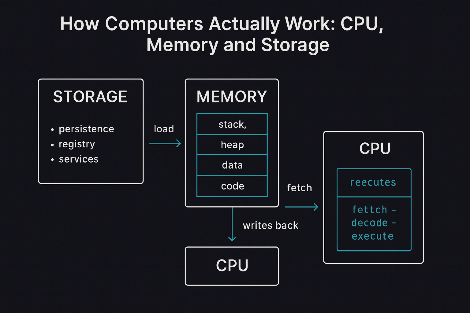
How They Work Together
The CPU, Memory, and Storage work in a coordinated fashion to enable a computer to perform tasks.
- When you open an application or file, the operating system retrieves the necessary data and instructions from Storage.
- This data is then loaded into RAM for quick access by the CPU.
- The CPU fetches instructions and data from RAM, processes them, and performs the required calculations.
- If the CPU needs to save changes or access additional data, it interacts with RAM.
- Once you save a file or close an application, the updated data is written back to Storage for long-term retention.
Path:
[Storage: binary file]
↓
[Memory: loaded into process space]
↓
[CPU: executes instructions]
↓
[Memory: results, buffers, logs]
↓
[Storage: saved output or persistence]
Relevance of Low-Level Understanding to Reverse Engineering
This architectural understanding provides critical context for dynamic and static analysis:
- Exploit Development and Analysis: Knowing the physical memory map (e.g., MMIO regions, BIOS ROM location) and low-level communication protocols (PCIe, DMI) is essential for developing or analyzing exploits that target the kernel or firmware (e.g., rootkits, bootkits).
- Performance and Timing: Understanding the memory hierarchy (caches, IMC, dual-channel) directly informs why certain code sequences are fast or slow. This is crucial for analyzing and exploiting side-channel attacks (like Spectre, Meltdown, or RowHammer).
- Persistence and Stealth: Malware persistence often occurs at the lowest layers - firmware (UEFI/BIOS), boot sectors (MBR), or as device drivers via PCIe. Forensic analysis of these layers is impossible without knowledge of the hardware initialization path.
- Debugging Abstraction: The debugger (like x64dbg or IDA Pro) abstracts hardware away, showing you only registers and virtual memory. A true reverse engineer understands that every MOV instruction is a potential cache-line load/store and every stack operation is a physically managed DRAM transaction. By stripping away the OS and debugger abstractions, you gain a clearer picture of intent.